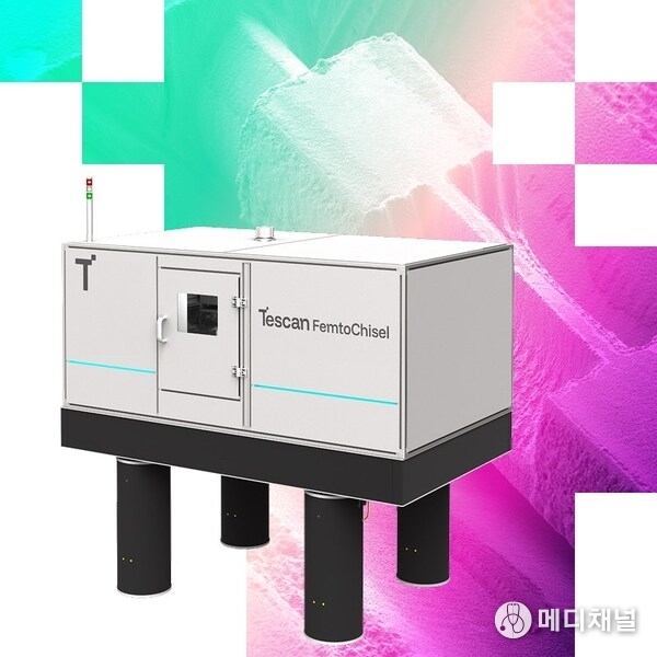
BRNO, Czech Republic, Nov. 14, 2025 -- Tescan expands its semiconductor portfolio with FemtoChisel, a next-generation femtosecond laser platform designed to enhance semiconductor sample preparation workflows with exceptional speed, precision, reproducibility, and quality.

FemtoChisel was developed specifically for semiconductor research and failure analysis environments where both throughput and adaptability are critical. By combining nanometer-level precision and high-throughput intelligent laser processing, FemtoChisel delivers pristine surfaces while significantly reducing the need for subsequent FIB polishing steps. This enables faster turnaround in research and failure analysis for current, and future, semiconductor materials.
"Semiconductor research and failure analysis teams are under constant pressure to deliver faster, more reliable results from any material layer within semiconductors stack. With FemtoChisel, we've addressed this challenge in our Large Volume Workflow for Semiconductors," said Sirine Assaf, Chief Revenue Officer at Tescan." It's not just a new instrument – it's a workflow enabler. By integrating ultrafast, femtosecond laser precision with intelligent adaptive laser processing, we're helping labs accelerate sample preparation, reduce rework, and bring clarity to increasingly more complex devices."
Workflow benefits of FemtoChisel include
- Adaptive multi-material processing, High Fluence Laser Machining with proprietary intelligent multi-gas processing and laser protective layer that preserves device integrity across metals, polymers, and advanced packaging stacks.
- High-throughput access to buried structures with taper-corrected, debris-free cross-sections – often eliminating the need for FIB fine polishing.
- Selective backside thinning with mirror-like surfaces (Ra < 0.4 µm), enabling optical fault analysis without artifacts.
- Large-area delayering (> 5 mm) with automated endpointing for accurate layer-by-layer removal at laser speeds.
- By uniting laser processing, electron microscopy, and FIB into complementary workflows, Tescan is helping semiconductor innovators overcome traditional bottlenecks in sample preparation. FemtoChisel serves both recipe-driven environments and flexible research in advanced packaging and R&D labs, providing a versatile solution for current and future semiconductor demands.
Tescan's commitment to integrated workflows is further strengthened by its Laser Technology Business Unit, established following the acquisition of FemtoInnovations. This dedicated focus ensures continued innovation in laser-enabled sample preparation technologies for the semiconductor industry.
About Tescan
Tescan enables nanoscale investigation and analysis within the materials and geosciences, life sciences, and semiconductor industries. With innovation scanning electron microscopy, FIB, and femtosecond laser technologies, Tescan delivers workflow solutions that accelerate discovery and problem-solving for academic institutions, industry leaders, and research labs worldwide.

